Design Considerations for Flexible PCBs
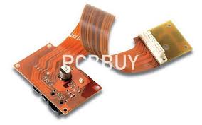
Flexible PCBs
A flexible printed circuit board (FPC) is an insulating material with conductive traces etched or printed on it. Unlike rigid PCBs, FPCs can be shaped to fit tight spaces and move dynamically. These attributes make them a key component in devices like mobile phones and medical equipment that require many connections in a compact space. FPCs are also durable, making them a great choice for high-performance and rugged applications.
When designing a fpc pcb, there are several design considerations that should be taken into account. First, consider the target environment and use conditions. This information will inform all construction decisions. Then, choose the appropriate materials for flexibility and durability. Polyimide is the most common choice for flexibility, allowing for tighter bend radii and excellent resistance to chemicals. Polyester is a good alternative to polyimide for lower cost and temperature ratings. PEN is a thinner option that allows for tighter bend radii and better ductility. Finally, be sure to choose a material that is compatible with wave soldering.
Since a flex circuit is made of multiple layers, the layout must be carefully planned to avoid delamination. This condition occurs when the underlying layers detach from one another, resulting in abrupt damage to the circuitry. To prevent this, designers should use strategic layer stacking to minimize the number of exposed layers. They should also avoid routing on layers that might drop out, using curved corners instead of orthogonal routes.
Design Considerations for Flexible PCBs
Another important design consideration is how to disperse heat throughout the circuit board. If a component generates a lot of heat, it is essential to place it away from other components that are sensitive to it. This will help to keep the overall board temperature down and prevent thermal shock, which can damage components. Additionally, it is a good idea to include thermal relief pads on the vias that connect to the ground plane. This will allow heat to conduct to the ground plane rather than remaining trapped near the surface of the flex.
The next step is to develop the schematic, highlighting critical traces and connections. It is a good idea to use FEA tools to simulate flexing and analyze the expected bending, fatigue, and failure risks. This will help to identify high-risk areas, and allow designers to plan accordingly. Once the schematic is completed, the final product can be assembled by a PCB manufacturer. This includes the placement of the flex components, mounting of the conductive pads, and attaching of the external terminals or pins. The final product should be tested for proper operation.
To ensure that a flex circuit can handle the rigors of its application, it must be designed with the correct materials. It is a good idea to use adhesives that can withstand the temperature range of the device, and to choose a material that is resistant to acids, oils, and UV exposure. It is also important to use proper construction techniques to limit the amount of stress that can be placed on the flex circuit during operation.